

High-Speed Board Design: In the modern world, the complexity of electronic products has increased due to the demand for higher performance such as faster data transfers, better image processing, higher computing power, and greater functionality.
As a result, PCBs now have higher signal frequencies (Multi GHz), more high-speed interfaces (such as PCIe Gen 4/5/6, DDR-3/4/5, USB HS/SS, Multi-Gig Ethernet), HDI (High-Density Interconnect), and increasingly use complex via types including Micro/Blind/Buried vias in PCB design.
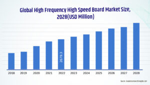
According to Business Research Insights, the size of the high-frequency high-speed board market worldwide in 2022 was 2679.3 million USD.
Based on the analysis, the market is anticipated to grow at a compound annual growth rate (CAGR) of 11.4% to reach USD 5120.8 million in 2028.
In the future, PCBs will need to handle increasingly larger component densities and operating speeds due to the demand for ever-higher performance and miniaturization from computers, smartphones, and communication devices.
To ensure that the design will function correctly, many variables and parameters must be carefully chosen while creating a high-speed PCB.
We’ll cover the major aspects of designing a high-speed PCB in this article, along with all the things that you should know.
What is a High-Speed PCB design?
When signals on a printed circuit board (PCB) have fast edge rates, they tend to be influenced by even the minute details in the PCB design.
Physical parameters including board stack-up, impedance, loop area, general design, and package type might cause these signals to lose integrity.
Thus, high-speed PCB design involves all the design techniques that are optimized to maintain signal integrity for these rapidly changing signals.
When a design is High-Speed?
Whether a board design is in the low-speed or high-speed design regime is determined by the rise time of its signals.
The max frequency (Fmax) contained in a digital signal is dependent upon the rise time of the signal and is related as per the below equation,
Fmax = 0.35/Tr
where Tr = rise time of the signal
Broadly speaking, high-speed PCB design requirements should concern you if the signal’s rise time is less than 5 ns, which roughly corresponds to Fmax of 70MHz or more.
Furthermore, the concepts of the Transmission Line effect, become prominent when the time required for a signal to travel along a trace is longer than approximately one-quarter of the signal rise time.
For such high-speed signals, the concepts related to signal integrity need to be properly followed.
Key Concepts in High-Speed PCB Design
Signal Integrity (SI)
- A simpler term for “signal integrity” is the confidence and quality of signals passing through a PCB. To maintain this, there should be no reflections, crosstalk, ground bounce, etc.
- Signal reflections occur due to impedance mismatches leading to some part of the signal being reflected to the source.
- Conversely, crosstalk refers to the undesired coupling of signals coming from adjacent traces leading to noise or even other disturbances.
Impedance Control
- Impedance Control is the process of keeping the impedance of PCB traces even to avoid signal reflection and signal loss.
- The high-frequency signals especially require this, since any slight changes in impedance cause considerable signal degradation.
- The main concern in impedance control is the calculation as well as regulation of trace widths
Timing and Skew
- Timing Machine synchronization, only synchronized systems can guarantee signal cohesion..start Date arrives after endDate (signals for endDate should reach the right time).
- We can have the confidence that timing and delay are appropriate for the functions of high-speed circuits only if certain requirements are met.
Electromagnetic Interference (EMI)
- Unwanted interference from electromagnetic radiation emitted by electronic parts is known as EMI.
- PCB cannot exude too much electromagnetic radiation or become overly vulnerable to its influence without controlling EMI.
- This includes employing correct layout tactics, filtering, and shielding.
High-Speed PCB Design Challenges and Considerations
The design challenges that arise while creating high-speed printed circuit boards are outlined in this section,
Signal Integrity
The quality of high-speed signals can be lowered by noise, reflection, and distortion. Among the things to keep in mind when preserving signal integrity are,
- Impedance Control – Controlled impedance traces help to maintain constant impedance along the signal channels.
- Termination – Utilize suitable termination methods (such as series or parallel termination) to minimize reflections by matching the source and load’s impedances.
- Short Trace Lengths – To minimize the possibility of signal degradation and to reduce latency, keep traces as short as feasible.
Electromagnetic Interference (EMI)
The performance of the PCB and adjacent components may be impacted by high-speed signals’ potential to produce electromagnetic interference and to be vulnerable to it.
Key considerations in containing this challenge are
- Shielding – To prevent outside interference from reaching sensitive communications, use shielding techniques and ground planes.
- Filtering – To reduce EMI, including capacitors, ferrite beads, and other filtering elements.
- Trace Layout – To reduce crosstalk and EMI, avoid running high-speed traces parallel to one another.
Crosstalk
Crosstalk is the result of adjacent traces’ signals interfering with one another, corrupting data. Important strategies for addressing crosstalk include:
- Trace Spacing – Radius up the high-speed traces to minimize inductive and capacitive coupling.
- Ground Planes – To reduce crosstalk and give signals a return path, use solid ground planes.
- Differential Pairs – For high-speed data connections, use differential signaling to minimize crosstalk and cancel out noise.
Power Integrity
Performance maintenance depends on clean, steady power delivery to high-speed components. Important things to keep in mind when preserving power integrity are,
- Decoupling Capacitors – To reduce noise and offer a steady power supply, place decoupling capacitors adjacent to the power pins of high-speed integrated circuits.
- Power Planes – When distributing power, use specialized power planes to provide low-impedance pathways.
- Power Integrity Analysis – To find any problems and improve the power distribution network, do a power integrity study.
Layer Stackup Design
Managing power distribution, thermal performance, and signal integrity all depend on designing the right layer stack up.
It is necessary to strike an appropriate balance between PCB cost and design specifications. Important factors are,
- Layer Count – To keep power, ground planes, and high-speed signals apart, use an adequate number of layers.
- Material Selection – Select materials that can facilitate the transmission of high-speed signals by having the right dielectric characteristics.
If there is a lot of heat dissipation in the design, take thermal performance into account as well. The conventional fiberglass based on FR4 is not the greatest for creating high-speed PCBs. PCB materials for high-speed designs include polyamide, PTFE, and improved FR-4.
Megatron 6 and Rogers 4350B, two low-loss materials with low dissipation factor (Df) and dielectric constant (Dk) values, are commonly utilized in high-speed PCB materials.
- Symmetrical Stackup – To keep mechanical stability and avoid warping, make sure the layer stack-up is symmetrical.
Layout and Routing
Minimizing signal deterioration and guaranteeing dependable performance requires careful planning and routing. Important things to note are,
- Length Matching – Timing consistency is ensured by matching the lengths of essential signal routes and differential pairings.
- Via Minimization – To minimize signal reflections and loss, utilize as few vias as possible in high-speed signal pathways.
- Routing Guidelines – For high-speed routing and layout, abide by design requirements and industry best practices.
Thermal Management
Significant heat generation from high-speed components can hurt dependability and performance.
Heat dissipation and maintaining ideal operating temperatures are essential. Important things to think about when managing heat are
- Thermal Vias – To move heat from heated components to the ground plane or heat sink, use thermal vias.
- Heat Sinks and Fans – To disperse heat, include fans, heat sinks, and other cooling devices.
- Thermal Analysis – To find hotspots and make sure all high-speed components are adequately cooled, do a thermal analysis.
Design Verification
Verifying the design as early in the process as feasible to make sure it satisfies all performance and reliability requirements. Doing so can prevent expensive delays and overstretching.
- Simulation Tools – To validate the design, use simulation techniques such as power integrity, thermal analysis, and signal integrity.
- Design Reviews – With cross-functional teams, conduct in-depth design reviews to identify any problems early in the process.
- Prototyping – To find and fix any problems with the board’s performance, DFM (Design for Manufacturability), DFA (Design for Assembly), DFT (Design for Testability), etc., build and test prototypes. Then just make plans for increased output.
Manufacturing Process Tolerances
Specifying tolerances accurately for PCB fabrication is crucial to ensure the board’s performance, reliability, and manufacturability.
Some of the key tolerances to be specified in Fabrication Instructions are
- Board Outline and Board Thickness
- Drilling and Via Tolerances
- Controlled Impedance Tolerances
- Plating Tolerance
Key ways of handling this challenge are,
- Use IPC Standards – Refer to IPC standards (e.g., IPC-6012, IPC-2221) for industry-accepted tolerance guidelines.
- Communicate with Manufacturers – Engage with your PCB manufacturer early in the design process to understand their capabilities and limitations.
- Balance Performance and Cost – Stricter tolerances can increase manufacturing complexity and cost. Find a balance that meets your needs without unnecessary cost penalties.
Detailed Insights
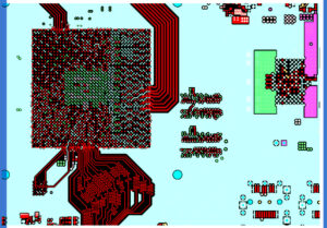
High-Speed PCB Routing
- As you route your design, the design guidelines you establish for your high-speed design project will guarantee that you fulfill the targets for length, spacing, and impedance.
- Furthermore, you can enforce critical differential pair routing criteria in your routine, such as minimizing length mismatches to prevent skew and enforcing trace spacing to guarantee that differential impedance targets are reached.
To guarantee performance, the best routing tools will let you codify your trace geometry limits as design rules.
Length tuning is used across parallel buses and between traces in differential pairs to ensure time delay matching and to eliminate the skew between signals seen at a receiver.
The positioning of ground planes near your traces is a critical aspect of high-speed PCB routing.
To provide consistent impedance and a specified return path in the PCB layout, the layer stack should be built using ground planes in layers next to impedance-controlled signals.
Avoid routing high-speed signals near noisy components or power traces. Route high-speed signals on internal layers between ground planes to shield them from EMI.
Further, it is not advisable to route traces over splits or gaps in the ground planes as this can result in an impedance discontinuity that causes an EMI issue.
Don’t Overlook the Return Path
This is one PCB high-speed design rule that many designers overlook. The return path that your board’s current takes in a real board deviates from the trace that carries the injected signal precisely below it.
Return currents are more likely to be restricted below the signal trace at higher speeds, but not at lower ones.
The following rules will assist in preventing excessive signal interference, EMI susceptibility, and power integrity issues:
- Avoid routing over gaps in the ground (or reference) plane. The gaps may be a result of anti-pads provided for Holes and vias or due to splits in the power plane. A high-speed signal should never be routed across these gaps. You raise the signal’s loop inductance by doing this. Due to this the trace’s impedance changes and it worsens transient ringing and crosstalk.
- Digital signals should not be routed across analog board segments. Since digital components are operating at saturation, digital signals are comparatively stable when subjected to interference from low-level analog signals. Analog signals do not work in the same way. Strong crosstalk between a digital signal and its return current in an analog signal on a mixed-signal board can seriously disrupt analog components. Hence, in your board analog and digital sections need to be properly planned.
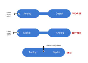
For mixed signal boards, to ensure that analog and digital signals do not interfere with one another, the high-speed PCB floor planning that is displayed above should be considered.
As long as the return path for each signal is appropriately identified, it is possible to keep the various signal types apart from one another by keeping the sections in different regions of the board.
Power Integrity
Power integrity is a wide subject that has a lot to do with high-speed PCB design.
In PCB design, ensuring steady power delivery to high-speed components is essential because power integrity issues might appear as signal integrity issues.
The transmission of very low-noise power to components is the main goal of power integrity. The primary determinants of power integrity in a digital design are the PCB stackup and the PDN layout.
If all goes according to plan, power rails will supply rapid digital components with very little noise and extremely mild transient oscillations.
Good power integrity design assures low emissions, low noise power delivery, and the removal of various SI issues common to high-speed interconnects.
Advanced Tools for High-Speed Design
All these features will be combined into one application by the best high-speed PCB design software, eliminating the need for you to employ distinct workflows to address various design issues.
To assure signal integrity, power integrity, and electromagnetic compatibility, high-speed PCB layout designers must put in a lot of work upfront.
However, with the correct tools, they can turn their findings into design guidelines that will guarantee the design works as intended.
Advanced PCB design software facilitates industry-standard analysis by integrating with simulation programs.
Certain simulation tools are designed with the express purpose of analyzing EMI in a PCB layout and assessing signal and power integrity in a new design.
In high-speed design, simulations are highly helpful since they allow users to identify specific SI/PI/EMI issues before a design is put into production.
Return path tracking, identifying an impedance discontinuity in traces, and strategically placing decoupling capacitors to avoid electromagnetic interference are a few instances.
Complete your physical layout with the best high-speed design software.
Use the greatest suite of high-speed design and layout tools based on a rules-driven design engine for developing sophisticated high-speed digital systems while making sure you preserve power and signal integrity.
The finest PCB layout tools will enable you to maintain your flexibility when designing your high-speed PCB layout, regardless of whether you need to plan a dense single-board computer or a complicated mixed-signal PCB.
Conclusion
PCB design strategies have evolved to overcome the difficulties posed by high-frequency and high-speed applications.
High-performance printed circuit boards are a result of several key aspects, including stack-up design, efficient signal routing, material selection, and sophisticated design tools and methodologies.
As outlined in this article, PCB designers must constantly create and implement cutting-edge PCB design methodologies to keep up with increasing technological demands.