Introduction
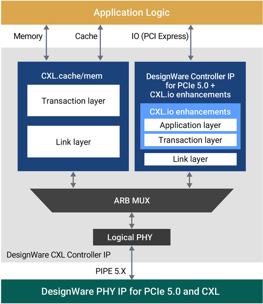
The PCIe 5.0 standard’s PCIe, 5.0 PHY at 32 GT/s, is used to convey the three protocols that the CXL standard provides.
To provide shallow latency paths for memory access and coherent caching between host processors and devices that need to share memory resources, like accelerators and memory expanders, the Compute Express Link standard addresses some of these limitations by leveraging the PCIe 5.0 physical layer and electrical.
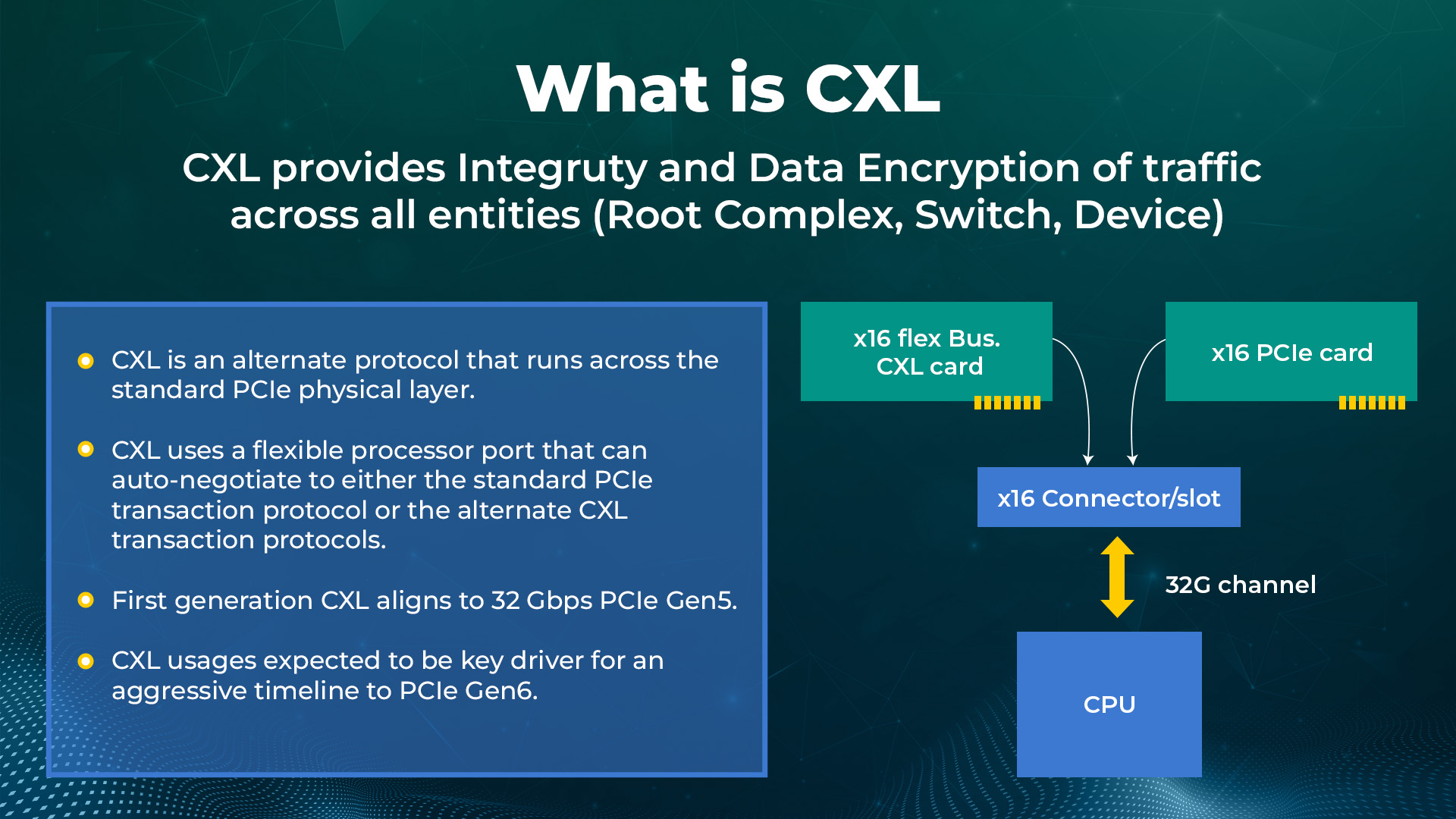
The supported standard modes for CXL are centered around a PCIe 5.0 PHY running at 32 GT/s in an x16 lane. 32GT/s is also enabled in x8 and x4 lane configurations to enable bifurcation.
Degraded modes are not expected to be widespread in target applications and are defined as anything narrower than x4 or slower than 32GT/s.
While Compute Express Link can provide significant performance benefits for many applications, specific devices only require signaling task submission and completion events, frequently when working with oversized data items or contiguous streams.
What is CXL
Compute Express Link (CXL), an open industry standard memory connection. It offers fast connectivity between the many forms of memory utilized in modern data centers, including CPUs, TPUs, GPUs, and other processor types.
Intensive workloads for CPUs and purpose-built accelerators are the focus of Compute Express Link, and a new open interconnect standard enables efficient and coherent memory access between a host and a device.

Recently, the Compute Express Link 1.0 specification was released along with the announcement of a consortium to enable this new standard.
To decide how to best leverage and incorporate this new interconnect technology into their designs for AI, machine learning, and cloud computing applications, system-on-chip (SoC) designers need to be aware of some of the significant Compute Express Link features that are described in this article.
Compute Express Link is an open-source interconnect that links memory to server and storage processing. Its primary advantage over current practices is the potential for building memory pools with significantly higher capacities than currently accessible.
Additionally, it enables the creation of pools of memory composed of components from many vendors that may be directly connected to processors in the CPU, GPU, and DPU form factors, as well as to smart NICs and computational storage.
This is so that a pool can establish a cache for working datasets using Compute Express Link, an open-source memory interface that is supposed to be universal.
It has emerged due to the failure of storage-class memory to keep up with the demands of the increase in numerous processing nodes in terms of product and technological innovation.
The challenge of getting SCM to function with these modules created a need for something simpler from which to construct memory pools. Compute Express Link provides that capability.
Features and Benefits of CXL
The performance and efficiency of computing are significantly increased while TCO is decreased by streamlining and enhancing low-latency networking and memory coherency.
Beyond the constrained DIMM slots in today’s servers, Compute Express Link memory extension options allow more capacity and bandwidth. Through a CXL-attached device, Compute Express Link enables the addition of extra memory to a CPU host processor.
The low-latency Compute Express Link link enables the CPU host to use this additional memory in addition to DRAM memory when combined with persistent memory. Reasonable memory capacity workloads, like AI, are dependent on high performance.
The benefits of CXL are apparent when you consider the workloads that most companies and data center operators are investing in.
Compute Express Link Specification:
The Compute Express Link Specification 1.0 based on PCIe 5.0 was released on March 11, 2019. A coherent cache protocol enables the host CPU to access shared memory on accelerator devices. In June 2019, the CXL Specification 1.1 was released.
The CXL Specification 2.0 was issued on November 10, 2020. The updated version implements device integrity and data encryption as well as CXL switching, which enables connecting multiple Compute Express Link 1. x and 2.0 devices to a CXL 2.0 host processor and pooling each device to multiple host processors in distributed shared memory and disaggregated storage configurations.
Because CXL 2.0 continues to use PCIe 5.0 PHY, there is no bandwidth gain from Compute Express Link 1. x.
The PCIe 6.0 PHY-based next edition of Compute Express Link standards is anticipated in H1 2022.
Future of CXL
The usage of many protocols in large systems with memory coherency to support CPU-to-CPU, CPU-to-attached devices, and longer-distance chassis-to-chassis requirements is conceivable.
Compute Express Link is concentrated on server-optimized solutions. Due to its asymmetry, it might not be the best for CPU-to-CPU or accelerator-to-accelerator connections.
An alternate transport might be more appropriate to enhance performance for rack-to-rack setups due to its reliance on PCI 5.0 PHYs.
Since Compute Express Link and PCIe 5.0 are closely related, we anticipate that CXL-compatible products will be released simultaneously as PCIe 5.0.
According to an editorial published on March 11, 2019, Intel “plans to release devices that utilize Compute Express Link technology starting in Intel’s 2021 data centre platforms, including Intel® Xeon® processors, FPGAs, GPUs, and SmartNICs.” 2
To aid in adopting the standard, the Compute Express Link consortium has acknowledged the necessity to establish some type of interoperability and compliance program.
As a result, a few minor changes will be made to the specification to meet this requirement, and eventually, it seems likely that a compliance program will be implemented.
The market for Compute Express Link Controller IP is expected to be worth USD million in 2022 and is predicted to grow at a CAGR during the review period to become USD million by 2028.
At a CAGR over the forecast period, the size of the Compute Express Link Controller IP market in the United States is anticipated to increase from USD million in 2021 to USD million by 2028.

What is PCIe Gen 5
PCIe 5 is a new PCI Express standard that improves upon PCIe 4.0 in several ways. The upcoming standard for computer peripherals is PCIe Gen 5.
In 2022 and beyond, you’ll hear a lot about PCIe 5.0 because Intel already has the Alder Lake architecture to enable it.
PCIe 5.0 will also be supported by AMD’s next Ryzen 7000 series, which is anticipated to launch before the end of 2022.
Although PCIe 5.0’s official announcement didn’t occur until May 2019, its rough specification was released in 2017.
Speed and bandwidth are two critical distinctions between each PCIe iteration. With a bandwidth of 8 GB/s and a transmission rate of 2.5 GT/s, PCIe Gen 1 launched everything.
We’re looking at transfer rates of up to 32 GT/s and bandwidth of up to 128GB/s across an x16 configuration. This ought to help you understand how much the standard has changed.
We’re looking at 64GB/s throughput across an x16 lane connection for PCIe 5.0 support on Intel Alder Lake. In addition to an additional x4 PCIe 4.0 connection, the high-end AlderLake-S chips offer an x16 PCIe 5.0 connection.
One of the main issues with the current generation of graphics cards is power delivery, which is another intriguing issue that PCIe 5.0 is intended to address. Yes, they can provide adequate power for powerful graphics cards. Only 150W per 8-pin connector may currently be supplied.
Due to this, you require two, occasionally even three, of those connectors. However, the new 16-pin PCIe 5.- connection will have adequate power to operate.
Features and benefits of PCIe 5
Despite having twice the speed of PCIe 4.0, PCIe 5.0 still supports older devices.
Our PCIe, gen-5 protocol analyzers, can capture higher volume upstream and downstream traffic at 32 GT/sec data link speeds and better memory, storage capacity, and segmentation.
PCIe Gen 5 Specification
The PCIe 5.0 specification, which does not include any intrinsic link or transaction layer changes, can be categorised as a natural progression of the backwards-compatible PCIe standard.
The expanded tags and credits introduced with PCIe 4.0 and the scaled flow management continue to be advantageous to the PCIe 5.0 specification.
A new CEM connector made specifically for add-in cards has also been included. Overall performance and reliability have increased as a result of improvements to signal integrity and connector design features.
EIEOS, SKP ordered sets, and equalization sequence updates are the physical layer improvements.
Hardware makers and industry insiders have primarily praised the PCI Express 5.0 specification.
The improvements to increase testability, speed uplink training, and support alternative protocols have all been acknowledged as outstanding PCIe 5.0 qualities.
This industry consensus has been the driving force behind the ambitious hardware development and commercialisation goals and the comparatively uncomplicated implementation requirements needed to upgrade from PCIe 4.0 to PCIe 5.0.
The Future of PCIe 5.0
With the final specification release for PCIe 6.0 anticipated in 2021, the rapid pace of PCIe release dates appears to continue.
With a stunning 256 GB/sec of bidirectional capacity, this latest generation will maintain the PCIe standard’s heritage of bandwidth doubling and backward compatibility. As a result, PCIe will practically match the VRAM bandwidth of a low-end GPU.
Pulse amplitude modulation (PAM4) and forward error correction (FEC) technology will be integrated to allow another two-fold speed boost while maintaining high-reliability standards.
Artificial intelligence and machine learning could benefit from this improvement as their performance depends on outstanding speed, low latency, and quick access to numerous peripherals at once.
Another successful advancement in I/O busing technology is PCIe Gen 5. For the foreseeable future, the PCIe 5.0 specification will keep up with Moore’s law while letting networking design take the bottleneck role.
This development should successfully continue through the release of PCIe 6.0, and many additional subsequent generations as new and enhanced PCIe 5.0 test tools are being developed daily.
According to Technavio’s analysis, the PCI express market is expected to increase by USD 20.29 billion between 2020 and 2024, expanding at a CAGR of over 26%.

Why PCLe 5.0 and CXL?
Communication protocols have made significant advancements in the semiconductor sector.
The device-to-device performance required for cloud-based workloads, artificial intelligence, and machine learning applications is provided by the PCIe Gen 5 (and Gen 6, whose version 1.0 is scheduled for 2021) standard.
The central processing unit (CPU)-to-device and CPU-to-memory communication provided by the rapidly growing CXL standard enables next-generation data centre performance.
Both are essential next-generation system enablers that need support in the form of semiconductor intellectual property (IP) to be implemented.
It is unusual for PLDA to announce key accomplishments for PCIe and CXL simultaneously.
- One demonstrates successful PCIe 5.0 link training with PLDA’s PCIe 5.0 controller and Broadcom’s PHY.
- The other is successful CXL interoperability with the pre-production Intel Xeon CPU, code-named Sapphire Rapids.

Conclusion
The CXL standard, which appears to be gaining ground quickly, has advantages for devices that must effectively process data while coherently sharing memory with a host CPU.
The CXL consortium has 75 members as of this article and is continually expanding. With Intel, a large CPU manufacturer, supporting the standard and introducing CXL-capable devices in 2021, it appears likely that there will be widespread industry acceptance.
As you can see, PCIe 5.0 is still in its infancy. Although Intel’s Alder Lake architecture supports this new standard and its peripherals, we believe it will be some time before these new peripherals are available.
Although PCIe 5.0 peripherals will be pricey, they are predicted to appear just before AMD’s Ryzen 7000 series CPUs launch. We believe that until the new goods are widely available, most buyers interested in purchasing even a high-end enthusiast PC will be better off sticking with Gen 4 items.


